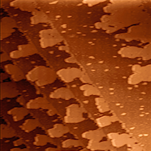
غشاء رقيق
الغشاء الرقيق thin film، هو طبقة من مادة يتراوح سمك قطعها من النانومتر (طبقة أحادية) إلى عدة ميكرومترات. تستخدم بشكل رئيسي في أجهزة أشباه الموصلات الإلكترونية والطلاءات البصرية.
التطبيق الشائع للأغشية الرقيقة هي المرايا المنزلية، والتي عادة ما تطلى بطبقة معدنية رقيقة على خلفية اللوح الزجاجي لتشكيل الواجهة العاكسة. كانت عملية تفضيض الزجاج شائعة لتصنيع المرايا. يستخدم الطلاء بالأغشية بالغة الرقة (بسماكة أقل من 50 نانومتر) لصنع المرايا المزدوجة.
عملية الطلاء البصري (مثل المضاد للانعكاس) عادة ما تكون أفضل عندما يتكون طلاء الغشاء الرقيق من عدة طبقات ذات السماكة ومؤشر انكسار مختلف. بالمثل، فالبنية الدورية للاستخدام المتناوب الأغشية الرقيقية المصنوعة من خامات مختلفة قد تشكل معاً ما يعرف بالشبكة الفائقة والتي تستخدم ظاهرة التقييد الكمومي بتقييدها الظاهرة الإلكترونيية في اتجاهيين.
العمل بالأغشية الرقيقة المغناطيسية الحديدية والكهربائية الحديدية[1] يستخدم كذاكرة الحاسوب. يتم تطبيقه أيضاً في الأدوية، في صورة الأدوية معبأة في شرائط. تستخدم الأغشية الرقيقة لتصنيع بطاريات الغشاء الرقيق والخلايا الشمسية من الغشاء الرقيق.
الأغشية الرقيقة الخزفية واسعة الاستخدام. الصلابة والخمول المرتفع نسبياً للمواد الخزفية يجعل هذا النوع من الطلاء الرقيق مفيداً لحماية المواد الأساسية من التآكل، الأكسدة والاحتكاك.
التنوي
Nucleation is an important step in growth that helps determine the final structure of a thin film. Many growth methods rely on nucleation control such as atomic-layer epitaxy (atomic layer deposition). Nucleation can be modeled by characterizing surface process of adsorption, desorption, and surface diffusion.[2]
Adsorption and desorption
Adsorption is the interaction of a vapor atom or molecule with a substrate surface. The interaction is characterized the sticking coefficient, the fraction of incoming species thermally equilibrated with the surface. Desorption reverses adsorption where a previously adsorbed molecule overcomes the bounding energy and leaves the substrate surface.
The two types of adsorptions, physisorption and chemisorption, are distinguished by the strength of atomic interactions. Physisorption describes the Van der Waals bonding between a stretched or bent molecule and the surface characterized by adsorption energy . Evaporated molecules rapidly lose kinetic energy and reduces its free energy by bonding with surface atoms. Chemisorption describes the strong electron transfer (ionic or covalent bond) of molecule with substrate atoms characterized by adsorption energy . The process of physi- and chemisorption can be visualized by the potential energy as a function of distance. The equilibrium distance for physisorption is further from the surface than chemisorption. The transition from physisorbed to chemisorbed states are governed by the effective energy barrier .[2]
Crystal surfaces have specific bonding sites with larger values that would preferentially be populated by vapor molecules to reduce the overall free energy. These stable sites are often found on step edges, vacancies and screw dislocations. After the most stable sites become filled, the adatom-adatom (vapor molecule) interaction becomes important.[3]
نماذج التنوي
Nucleation kinetics can be modeled considering only adsorption and desorption. First consider case where there are no mutual adatom interactions, no clustering or interaction with step edges.
The rate of change of adatom surface density , where is the net flux, is the mean surface lifetime prior to desorption and is the sticking coefficient:
Adsorption can also be modeled by different isotherms such as Langmuir model and BET model. The Langmuir model derives an equilibrium constant based on the adsorption reaction of vapor adatom with vacancy on the substrate surface. The BET model expands further and allows adatoms deposition on previously adsorbed adatoms without interaction between adjacent piles of atoms. The resulting derived surface coverage is in terms of the equilibrium vapor pressure and applied pressure.
Langmuir model where is the vapor pressure of adsorbed adatoms:
BET model where is the equilibrium vapor pressure of adsorbed adatoms and is the applied vapor pressure of adsorbed adatoms:
As an important note, surface crystallography and differ from the bulk to minimize the overall free electronic and bond energies due to the broken bonds at the surface. This can result in a new equilibrium position known as “selvedge”, where the parallel bulk lattice symmetry is preserved. This phenomenon can cause deviations from theoretical calculations of nucleation.[2]
Surface diffusion
Surface diffusion describes the lateral motion of adsorbed atoms moving between energy minima on the substrate surface. Diffusion most readily occurs between positions with lowest intervening potential barriers. Surface diffusion can be measured using glancing-angle ion scattering. The average time between events can be describes by:[2]
In addition to adatom migration, clusters of adatom can coalesce or deplete. Cluster coalescence through processes, such as Ostwald ripening and sintering, occur in response to reduce the total surface energy of the system. Ostwald repining describes the process in which islands of adatoms with various sizes grow into larger ones at the expense of smaller ones. Sintering is the coalescence mechanism when the islands contact and join.[2]
الترسيب
The act of applying a thin film to a surface is thin-film deposition – any technique for depositing a thin film of material onto a substrate or onto previously deposited layers. "Thin" is a relative term, but most deposition techniques control layer thickness within a few tens of nanometres. Molecular beam epitaxy, the Langmuir–Blodgett method, atomic layer deposition and molecular layer deposition allow a single layer of atoms or molecules to be deposited at a time.
It is useful in the manufacture of optics (for reflective, anti-reflective coatings or self-cleaning glass, for instance), electronics (layers of insulators, semiconductors, and conductors form integrated circuits), packaging (i.e., aluminium-coated PET film), and in contemporary art (see the work of Larry Bell). Similar processes are sometimes used where thickness is not important: for instance, the purification of copper by electroplating, and the deposition of silicon and enriched uranium by a CVD-like process after gas-phase processing.
Deposition techniques fall into two broad categories, depending on whether the process is primarily chemical or physical.[4]
الترسيب الكيميائي
الترسيب الفيزيائي
Physical deposition uses mechanical, electromechanical or thermodynamic means to produce a thin film of solid. An everyday example is the formation of frost. Since most engineering materials are held together by relatively high energies, and chemical reactions are not used to store these energies, commercial physical deposition systems tend to require a low-pressure vapor environment to function properly; most can be classified as physical vapor deposition (PVD).
The material to be deposited is placed in an energetic, entropic environment, so that particles of material escape its surface. Facing this source is a cooler surface which draws energy from these particles as they arrive, allowing them to form a solid layer. The whole system is kept in a vacuum deposition chamber, to allow the particles to travel as freely as possible. Since particles tend to follow a straight path, films deposited by physical means are commonly directional, rather than conformal.
Examples of physical deposition include:

A thermal evaporator that uses an electric resistance heater to melt the material and raise its vapor pressure to a useful range. This is done in a high vacuum, both to allow the vapor to reach the substrate without reacting with or scattering against other gas-phase atoms in the chamber, and reduce the incorporation of impurities from the residual gas in the vacuum chamber. Obviously, only materials with a much higher vapor pressure than the heating element can be deposited without contamination of the film. Molecular beam epitaxy is a particularly sophisticated form of thermal evaporation.
An electron beam evaporator fires a high-energy beam from an electron gun to boil a small spot of material; since the heating is not uniform, lower vapor pressure materials can be deposited. The beam is usually bent through an angle of 270° in order to ensure that the gun filament is not directly exposed to the evaporant flux. Typical deposition rates for electron beam evaporation range from 1 to 10 nanometres per second.
In molecular beam epitaxy (MBE), slow streams of an element can be directed at the substrate, so that material deposits one atomic layer at a time. Compounds such as gallium arsenide are usually deposited by repeatedly applying a layer of one element (i.e., gallium), then a layer of the other (i.e., arsenic), so that the process is chemical, as well as physical; this is known also as atomic layer deposition. If the precursors in use are organic, then the technique is called molecular layer deposition. The beam of material can be generated by either physical means (that is, by a furnace) or by a chemical reaction (chemical beam epitaxy).
Sputtering relies on a plasma (usually a noble gas, such as argon) to knock material from a "target" a few atoms at a time. The target can be kept at a relatively low temperature, since the process is not one of evaporation, making this one of the most flexible deposition techniques. It is especially useful for compounds or mixtures, where different components would otherwise tend to evaporate at different rates. Note, sputtering's step coverage is more or less conformal. It is also widely used in optical media. The manufacturing of all formats of CD, DVD, and BD are done with the help of this technique. It is a fast technique and also it provides a good thickness control. Presently, nitrogen and oxygen gases are also being used in sputtering.
Pulsed laser deposition systems work by an ablation process. Pulses of focused laser light vaporize the surface of the target material and convert it to plasma; this plasma usually reverts to a gas before it reaches the substrate.[6]
Cathodic arc deposition (arc-PVD) which is a kind of ion beam deposition where an electrical arc is created that literally blasts ions from the cathode. The arc has an extremely high power density resulting in a high level of ionization (30–100%), multiply charged ions, neutral particles, clusters and macro-particles (droplets). If a reactive gas is introduced during the evaporation process, dissociation, ionization and excitation can occur during interaction with the ion flux and a compound film will be deposited.
Electrohydrodynamic deposition (electrospray deposition) is a relatively new process of thin-film deposition. The liquid to be deposited, either in the form of nanoparticle solution or simply a solution, is fed to a small capillary nozzle (usually metallic) which is connected to a high voltage. The substrate on which the film has to be deposited is connected to ground. Through the influence of electric field, the liquid coming out of the nozzle takes a conical shape (Taylor cone) and at the apex of the cone a thin jet emanates which disintegrates into very fine and small positively charged droplets under the influence of Rayleigh charge limit. The droplets keep getting smaller and smaller and ultimately get deposited on the substrate as a uniform thin layer.
Growth modes
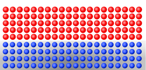
Frank–van der Merwe growth[7][8][9] ("layer-by-layer"). In this growth mode the adsorbate-surface and adsorbate-adsorbate interactions are balanced. This type of growth requires lattice matching, and hence considered an "ideal" growth mechanism.
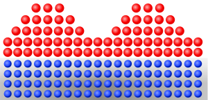
Stranski–Krastanov growth[10] ("joint islands" or "layer-plus-island"). In this growth mode the adsorbate-surface interactions are stronger than adsorbate-adsorbate interactions.
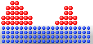
Volmer–Weber[11] ("isolated islands"). In this growth mode the adsorbate-adsorbate interactions are stronger than adsorbate-surface interactions, hence "islands" are formed right away.
Epitaxy
A subset of thin-film deposition processes and applications is focused on the so-called epitaxial growth of materials, the deposition of crystalline thin films that grow following the crystalline structure of the substrate. The term epitaxy comes from the Greek roots epi (ἐπί), meaning "above", and taxis (τάξις), meaning "an ordered manner". It can be translated as "arranging upon".
The term homoepitaxy refers to the specific case in which a film of the same material is grown on a crystalline substrate. This technology is used, for instance, to grow a film which is more pure than the substrate, has a lower density of defects, and to fabricate layers having different doping levels. Heteroepitaxy refers to the case in which the film being deposited is different from the substrate.
Techniques used for epitaxial growth of thin films include molecular beam epitaxy, chemical vapor deposition, and pulsed laser deposition.[12]
أنماط الإنتاج
البطاريات الفوتوڤولطية من الأغشية الرقيقة
بطاريات الأغشية الرقيقة
انظر أيضاً
المصادر
- ^ Thinfilm and InkTec awarded IDTechEx' Technical Development Manufacturing Award IDTechEx, April 15th 2009
- ^ أ ب ت ث ج Ohring, Milton (2002). Materials science of thin films : deposition and structure (2nd ed.). San Diego, CA: Academic Press. ISBN 9780125249751.
- ^ Venables, John A. (2000-08-31). Introduction to Surface and Thin Film Processes (1 ed.). Cambridge University Press. doi:10.1017/cbo9780511755651. ISBN 978-0-521-78500-6.
- ^ Knoll, Wolfgang Knoll; Advincula, Rigoberto C., eds. (2011-06-07). Functional Polymer Films, 2 Volume Set 1st Edition. Wiley-VCH. ISBN 978-3527321902.
- ^ Trontl, V. Mikšić; Pletikosić, I.; Milun, M.; Pervan, P.; Lazić, P.; Šokčević, D.; Brako, R. (2005-12-16). "Experimental and ab initio study of the structural and electronic properties of subnanometer thick Ag films on Pd(111)". Physical Review B. 72 (23): 235418. Bibcode:2005PhRvB..72w5418T. doi:10.1103/PhysRevB.72.235418.
- ^ Rashidian Vaziri, M. R.; Hajiesmaeilbaigi, F.; Maleki, M. H. (2011-08-24). "Monte Carlo simulation of the subsurface growth mode during pulsed laser deposition". Journal of Applied Physics. 110 (4): 043304. Bibcode:2011JAP...110d3304R. doi:10.1063/1.3624768.
- ^ Frank, Frederick Charles; van der Merwe, J. H. (1949-08-15). "One-dimensional dislocations. I. Static theory". Proceedings of the Royal Society of London. Series A, Mathematical and Physical Sciences. 198 (1053): 205–216. Bibcode:1949RSPSA.198..205F. doi:10.1098/rspa.1949.0095. JSTOR 98165.
- ^ Frank, Frederick Charles; van der Merwe, J. H. (1949-08-15). "One-Dimensional Dislocations. II. Misfitting Monolayers and Oriented Overgrowth". Proceedings of the Royal Society of London. Series A, Mathematical and Physical Sciences. 198 (1053): 216–225. Bibcode:1949RSPSA.198..216F. doi:10.1098/rspa.1949.0096. JSTOR 98166.
- ^ Frank, Frederick Charles; van der Merwe, J. H. (1949-08-15). "One-Dimensional Dislocations. III. Influence of the Second Harmonic Term in the Potential Representation, on the Properties of the Model". Proceedings of the Royal Society of London. Series A, Mathematical and Physical Sciences. 198 (1053): 125–134. Bibcode:1949RSPSA.200..125F. doi:10.1098/rspa.1949.0163. JSTOR 98394. S2CID 122413983.
- ^ Stranski, I. N.; Krastanov, L. (1938-02-10). "Zur Theorie der orientierten Ausscheidung von Ionenkristallen aufeinander". Monatshefte für Chemie und verwandte Teile anderer Wissenschaften. 146 (1): 351–364. doi:10.1007/BF01798103. ISSN 0343-7329. S2CID 93219029.
- ^ Volmer, M.; Weber, A. (1926-01-01). "Keimbildung in übersättigten Gebilden". Zeitschrift für Physikalische Chemie. 119U (1): 277–301. doi:10.1515/zpch-1926-11927. ISSN 0942-9352. S2CID 100018452.
- ^ Rashidian Vaziri, M. R.; Hajiesmaeilbaigi, F.; Maleki, M. H. (2010-10-07). "Microscopic description of the thermalization process during pulsed laser deposition of aluminium in the presence of argon background gas". Journal of Physics D: Applied Physics. 43 (42): 425205. Bibcode:2010JPhD...43P5205R. doi:10.1088/0022-3727/43/42/425205. ISSN 1361-6463. S2CID 120309363.
قراءات إضافية
كتب نصية
- M. Birkholz, with contributions by P.F. Fewster and C. Genzel (2005). Thin Film Analysis by X-Ray Scattering. Weinheim: Wiley-VCH. ISBN 978-3-527-31052-4. Table of contents
- M. Ohring (2001). Materials Science of Thin Films (2nd ed.). Boston: Academic Press. ISBN 9780125249751.
- K. Seshan, ed. (2012). Handbook of Thin Film Deposition (3rd ed.). Amsterdam: Elsevier. ISBN 978-1-4377-7873-1.
{{cite book}}:|author=has generic name (help)
تاريخية
- D.M. Mattox (2003). The Foundations of Vacuum Coating Technology. Norwich: Noyes / William Andrew Publishing. ISBN 0-8155-1495-6.
{{cite book}}: External link in|title=


![{\displaystyle n=J\sigma \tau _{a}\left[1-\exp \left({-t \over \tau _{a}}\right)\right]n=J\sigma \tau _{a}\left[\exp \left({-t \over \tau _{a}}\right)\right]}](https://www.marefa.org/api/rest_v1/media/math/render/svg/570cb89a89e841dcd45c2da0a0c4d4354fb05401)


![{\displaystyle \theta ={Xp \over (p_{e}-p)\left[1+(X-1){p \over p_{e}}\right]}}](https://www.marefa.org/api/rest_v1/media/math/render/svg/b51447b1d23955160e1b0e70fa79ac209bee2a8d)


